Micro-electromechanical system (MEMS) refers to a micro-device or system that can be manufactured in batches and integrates micro-structures, micro-sensors, micro-actuators, and signal processing and control circuits. Firstly, the interdigital electrode substrate prepared by MEMS technology has micro-nano-scale electrode spacing, which can greatly improve the signal-to-noise ratio, reduce the detection limit, and facilitate rapid response in seconds; secondly, the micro-electrode substrate based on MEMS technology The heater can achieve a lower heating power consumption in the milliwatt level and a temperature rise-fall rate in the millisecond level, which is conducive to the application of the sensor in the actual field. Based on MEMS technology, the size of the sensor can be greatly reduced, which is conducive to the sensor array architecture and the network monitoring of the sensor.
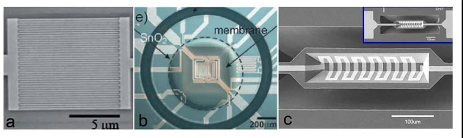
The MEMS substrate production process is currently relatively mature, and the difference between the sensor is mostly the integration method of the sensitive material and the substrate, mainly including atomic layer deposition method, electroplating method, thermal oxidation method, wet etching method, magnetron sputtering method and screen printing method Wait.
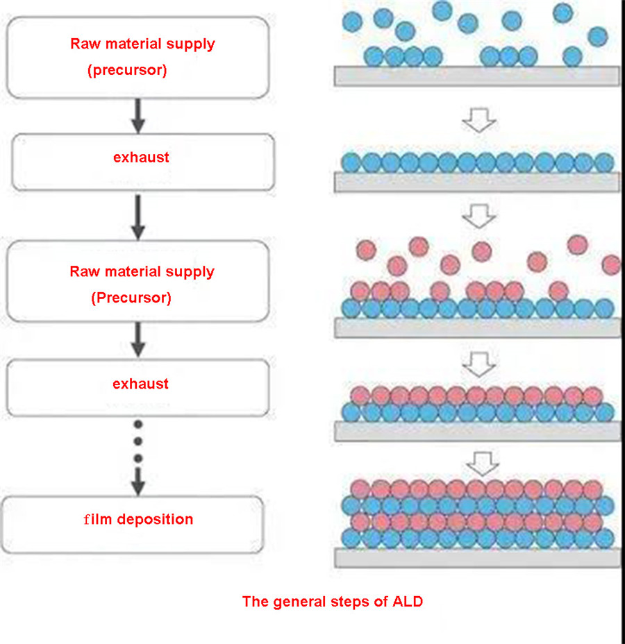
(1) Atomic layer deposition method
Atomic layer deposition (ALD) is a method in which a gas-phase precursor is repeatedly passed through the reactor and a deposited film is formed on the substrate. The precursor introduced each time will be deposited on the surface of the substrate and a thin film will be formed along with the surface reaction. After repeated cleaning and deposition, a thin film of the target thickness will be produced. Most of the metal oxide films and core-shell structures grown by atomic layer deposition can be used for sensing applications. By adopting this method, as long as there is a gap through which the film-forming material can pass, the film thickness can be controlled at the nanometer level. A uniform film is formed during processing.
(2) Electroplating method
Electroplating is the process of plating another layer of other metals or alloys on the surface of some metals using the principle of electrolysis. In the electroplating process, the plating metal is used as the anode and the target device is used as the cathode. The cations of the plating metal will be reduced on the surface of the workpiece to be plated to form a plating layer. The main advantage of electroplating technology is that it is an extremely cheap film preparation technology. In addition, electroplating technology can be used to prepare alloys, centimeter-level thick films and complex patterns, and electroplated films have good stress characteristics. Electroplating technology is limited by its own deposition principle, and generally requires a thin metal layer on the substrate as a seed (the so-called seed), so this limits the types of substrates to a certain extent.
(3) Thermal oxidation method
The main process of the thermal oxidation method: (1) the oxidant (O2/H20) reaches the surface of the silicon wafer in gaseous form; (2) the oxidant diffuses to Si in the solid medium (SiO2); (3) the oxidant reacts with Si. The film prepared by thermal oxidation method is denser than the film prepared by other methods. Thermal oxidation can be divided into dry oxidation and wet oxidation. The reaction temperature is 900~1200°C. The film obtained by dry oxidation is denser than that of wet oxidation.
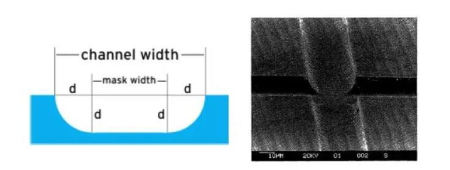
(4) Wet etching method
Wet etching is to produce regular topography on the surface of the material through a template and different etching agents. Different anisotropic etchants can etch different topography. A variety of three-dimensional silicon nanostructures can be produced by wet etching, such as nanowires, nanopillars and nanocones, sensors, vertical transistors, etc. In fact, most of these structures are made by reactive ion etching (RIE), which has high processing costs, low flux, and high fluorine pollution. Theoretically, wet anisotropic etching has clear and controllable characteristics, but it has not been well realized in practical applications. The reason is to a large extent that the chemical etchant will uniformly corrode the underlying substrate in all directions.
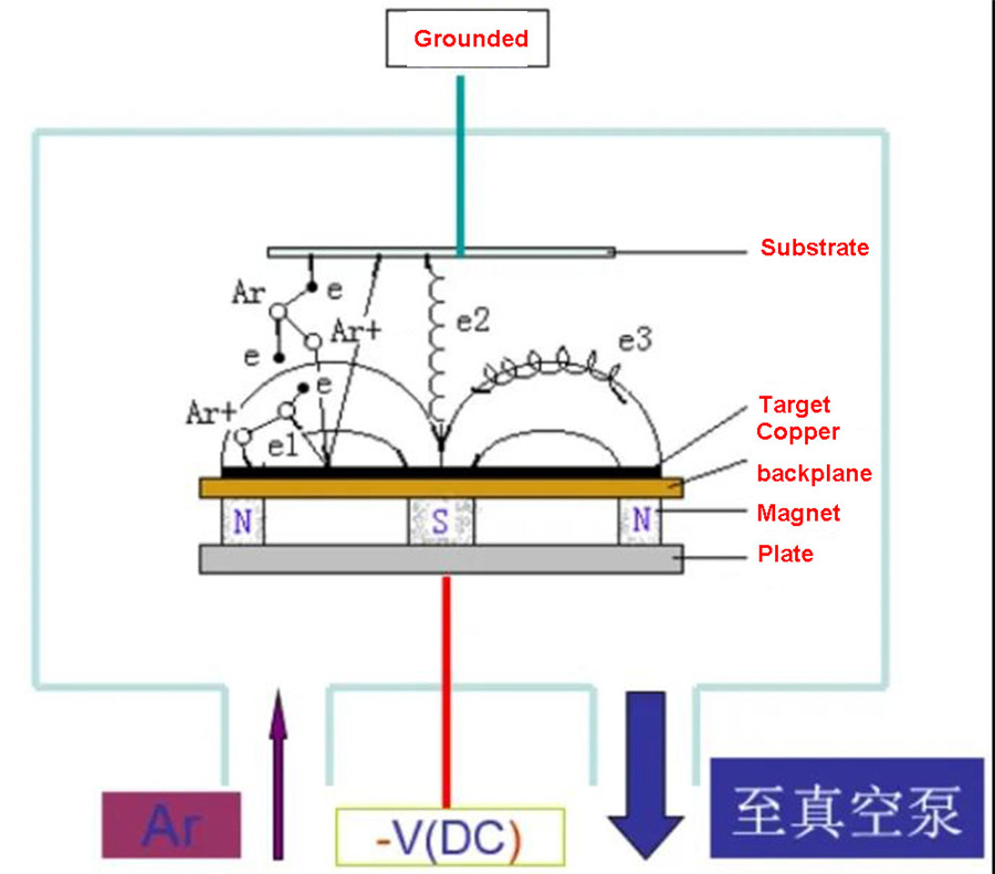
(5) Magnetron sputtering method
The principle of sputtering is to bombard the surface of the target with high-energy particles, bombarding atoms or molecules on the surface of the target, and hitting the substrate under the control of a magnetic field and an electric field to deposit a thin film. Magnetron sputtering is a type of physical vapor deposition (PVD), which is widely used to prepare thin films of various materials such as metals, semiconductors, and insulators. This method is simple to operate, easy to control, and has the advantages of strong adhesion and large coating area. Since its first development in the 1970s, magnetron sputtering technology has gradually been applied to industrial applications in the fields of decoration, semiconductor and manufacturing. At present, magnetron sputtering has become one of the most widely used and evolving technologies in the field of vacuum deposition. Compared with other sputtering technologies, magnetron sputtering can not only operate under lower pressure and relatively high deposition rate, but also can be used to synthesize dense films with less graininess.
So far, there have been some examples of MEMS sensors based on sputtered MOS films, including micromechanical WO3 sensors and sensing films containing p-n heterojunctions: SnO2-NiO films have high sensitivity to H2S at room temperature. However, the sensitivity of most sputtered films is still far lower than that of conventional chemically synthesized nanostructured MOS materials. This is because the amorphous and high-density structure limits the interaction between the sensitive material and the surrounding gas.
(6) Screen printing method
The development of screen printing technology has a very long history. It is a thick film technology that uses ink layer by layer to overlay a solid material, and uses screen frames or molds to change graphics. Because of its low cost and high efficiency , Mass production and other advantages are widely used in the fields of advertising production, poster printing, process production, and the use of screen printing technology to prepare sensors has become an important milestone. Compared with traditional rod-shaped electrodes, screen-printed electrodes can be integrated in various portable test systems due to their small size, and can directly contact and sense objects to be detected in the environment while avoiding operations such as sampling and transportation. The preparation process of screen-printed electrodes mainly consists of the following operating procedures, including graphic design, template formulation, material pretreatment, printing, and electrode drying. Electrodes are generally printed semi-automatically using a screen printer, or manually printed.
Sanyuan Industrial Zone, Xinzhan Area, Hefei, Anhui, China
Office in Shanghai: Room 602, Block E, Poly Plaza, Pudong, Shanghai, China
(24 Hours Customer Services)
Contact Person : Ryan Kang
MP : +82-10-4842-3326
Company Name : Respring Co.,Ltd
Contact Address : 3F, 133 Maean-ro, Haeryong-myeon, Suncheon-si, Jeollanam-do, ROK